K8 Scientific CMOS Camera


For Life Science Imaging Applications and Analysis
The K8 Scientific CMOS microscope camera offers a cutting-edge solution for the most challenging live-cell experiments. In an environment where sensitivity is everything, the K8 camera helps you capture more data* from your sample, thanks to a 95% quantum efficiency (QE) back-thinned CMOS sensor.
The K8 allows you to capture razor-sharp THUNDER images even in extreme low light imaging conditions, helping you to realize the full potential of your system. The K8 camera’s combination of extremely low read noise, minimal sensor artifacts and high QE allows you to extract quantifiable data from your sample while exposing it to the minimum of phototoxicity.
Gain the confidence to push the limits of your experiments with cutting edge sensor technology. Whether you need to capture stunning high-resolution images, carry out extreme low-light tracking of subcellular organelles or image high-speed cellular processes, the K8 can handle a wide range of challenging applications.
Capture more data* from your sample
Live cells respond by activating stress pathways when they are exposed to the high-intensity light that is typically used for fluorescent imaging.
The K8 camera’s increased camera sensitivity makes it possible to use lower light doses* to capture images, thus improving cell viability and allowing you to extract meaningful data from your sample for longer.
The K8 camera’s market-leading 95% QE sensor offers exceptional photon detection, allowing you to push your experiment further.
*Than achievable with legacy 80% QE CMOS cameras.
Razor-sharp THUNDER images even in extreme low light conditions
Unlike fixed samples, where users typically need to take a single image of a sample stained with photo stable dyes, live-cell imaging experiments require hundreds or even thousands of images of a photo sensitive sample to acquire a time lapse sequence. In order to get relevant results, it often becomes necessary to use much shorter exposures and lower excitation intensities to prevent photo damaging the sample, resulting in low signal to noise ratio (SNR) images.
The less light you work with on your samples, the lower the SNRs, and this is when the K8 camera truly displays its cutting-edge power, delivering razor sharp images even in extreme low light conditions. The K8 camera empowers your research through computationally enhanced THUNDER images with reduced artefacts at even lower light levels than previously possible.
Push the limits of your experiments
Take advantage of AI-enhanced clarity and accuracy enabled through the powerful combination of THUNDER and Aivia to analyze fluorescent images with greater accuracy, even when using low light excitation.
Leica offers a unique trilogy of technologies in the form of the K8 scientific CMOS microscope camera, THUNDER and Aivia that enables you to truly push the limits of your research while still extracting high quality quantifiable data from the images.
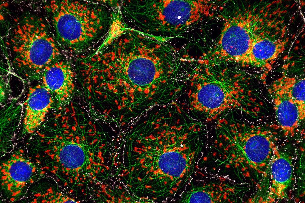
COS7 cells
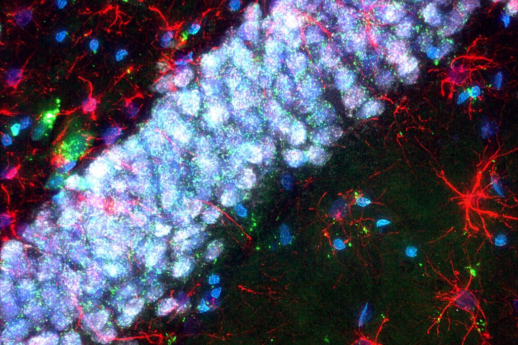
Rat brain
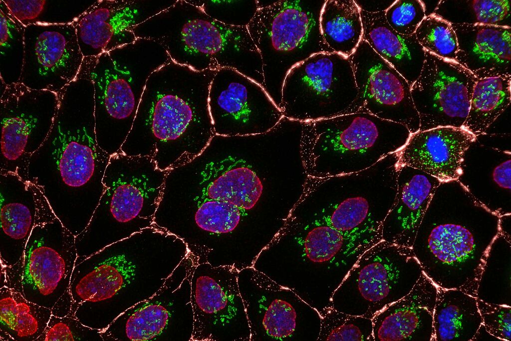
MDCK cells

THUNDER Imager Tissue
Explore the THUNDER Imager Tissue, which offers real-time 3D fluorescence imaging with computational clearing and is ideal for neuroscience, and histology.
DM4 B & DM6 B Upright Microscopes
Explore the Leica DM6 B microscope to enhance workflows with LAS X Navigator sCMOS imaging & intelligent automation for flexible applications. Order now!
THUNDER Imager Model Organism
THUNDER Imager simplifies screening and imaging of live model organisms like C. elegans and Drosophila with high-speed, blur-free z-stack capability.
Warranty Extension+
Protecting your investment upfront for complete peace of mind Designed to provide full system coverage for your newly purchased microscope and reduce the cost of ownership with exclusive rates. Delivering upon our commitment to extend your system’s lifetime and reduce risk with regular updates and checks. Key features 1-annual preventive maintenance 3-business day on-site response* Unlimited replacement of service parts All labor & travel costs included Required software updates & patches Proactive remote monitoring (RemoteCare)* 2-business hour approximate hotline response* *Varies by region or equipment
THUNDER Imager Cell Spinning Disk
Struggling to navigate complex samples? Discover the power of combining THUNDER technology with the CrestOptics CICERO spinning disk. This synergistic pairing allows you to get higher quality data and clearer details from 3D samples, delivering a deeper and more detailed view of your research.
DMi8 Inverted Microscope
Streamline your complex microscopy workflows with the DMi8 inverted microscope. The platform enables you to reliably generate high quality data with solutions that you can tailor to your research requirements and budget.
K3C & K3M The Microscope Camera K3 series
Explore K3M microscope cameras that deliver exceptional imaging for fluorescent samples, stained tissue & industrial materials with area scanning & stitching.